We all know how the recent global semiconductor crisis is disrupting every industry that has electronics at its core—automotive, gadgets, appliances, machinery, healthcare, and much more. Owing to that, they face multiple challenges like production delays, demand-supply gaps, and customer attritions. This crisis is a testimony to how electronics and their ecosystem remain a bedrock for many industries. While speaking of the essence of semiconductors, we should also look into the cruciality of PCBs. (Printed Circuit Boards).
Technically, PCBs are the physical platforms to which these semiconductors and other electronic components like resistors, capacitors, and integrated circuits are mounted. The PCB boards allow these electronic components to communicate and function seamlessly through conductive traces on the board.
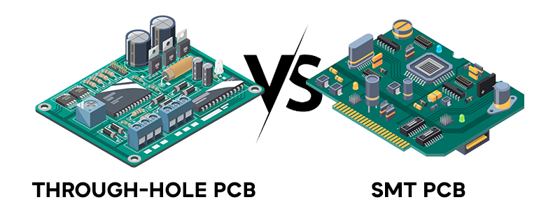
There are two primary methods for assembling PCBs: Surface Mount Technology (SMT) and Through-hole Technology.
SMT involves mounting components directly onto the surface of the PCB, while through-hole technology requires inserting components through holes in the board and then soldering it. Both assembly methods have their advantages and applications. In this blog, let us see the through-hole approach, its benefits, drawbacks, applications, and the exciting concept of SMT vs Through-hole assembly.
What is Through Hole Technology?
Before looking into what through-hole technology is, let us understand its history.
Through-hole technology, or thru-hole as it’s otherwise referred to, has a fascinating history that dates to the 1940s. Back then, people were drilling holes in PCBs, manually inserting components on one side, and soldering the leads on the other. It was a time-consuming process, but it laid the foundation for the evolution of through-hole technology.
So, what exactly is the through-hole approach?
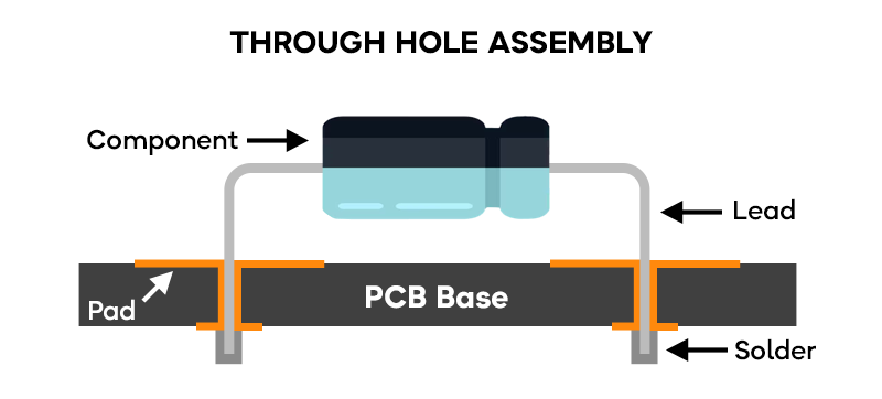
Through-hole technology is a method of electronic component assembly where components are inserted through holes drilled into a PCB. The component leads are soldered on the opposite side, creating a secure electrical and mechanical connection between the PCB and the component.
When you examine printed circuit boards (PCBs), you’ll notice numerous holes scattered across the surface of varying sizes. These holes can be divided into two main types: PTH (Plating Through Hole) and NPTH (Non-Plating Through Hole).
To tell them apart, take a close look at the hole walls. Suppose you see a layer of copper coating on the entire inner surface. In that case, you’re looking at a PTH, which is crucial for creating electrical connections between layers of the PCB and ensuring a smooth flow of current throughout the board.
On the other hand, an NPTH won’t have any copper lining the borehole walls, so they are primarily used for mechanical purposes rather than electrical connections.
Through-hole technology continues to be widely used, particularly in applications where durability and robustness are essential. That’s why you’ll often find through-hole components in products like cars, industrial equipment, and aerospace electronics.
So, next time you appreciate your sleek and powerful electronics, remember the humble beginnings of through-hole technology and the impressive evolution that has led us to where we are today. It’s a testament to the ingenuity and progress of the electronics industry!
Components and Processes in Through-Hole Technology
Now that you have a clear picture of through-hole assembly, let’s examine the through-hole electronic components and the process of assembling them into a PCB.
Through-hole Electronic Components
Through-hole technology involves using components with leads or pins designed to be inserted into holes on a PCB. Common through-hole components include resistors, capacitors, diodes, transistors, and integrated circuits (ICs). These components are typically larger than those found in surface-mount technology, making them easier to handle and solder manually.
Through-hole Technology Process
PCB Design & Manufacturing
A PCB layout and schematic diagram can be designed using CAD software with designated locations for components. This allows for precise placement of components on the PCB, ensuring proper functionality and connectivity. Computer numerical control (CNC) or manual drilling machines can accurately drill holes with specific diameters and depths at designated locations. Once drilled, the PCB is cleaned and coated with a flux layer to help the solder adhere to the board.
Then, the copper layer is applied over the board’s surface through electroplating, forming the conductive pathways for components. Attention to this layer is crucial during the PCB design and manufacturing process to ensure the reliable and efficient performance of the electronic device.
Component Placement & Insertion
The components are then placed into the pre-drilled holes on the PCB, with their leads protruding through the other side. Advancements in through-hole technology have significantly simplified the assembly process of electronic components. Now, we have automated insertion machines known as Through-Hole Component Insertion Machines or Through-Hole Inserters that can quickly place components in precisely drilled holes and secure them using lead clinching, ensuring reliable connections. This saves time and increases efficiency, making producing electronic devices on a large scale easier.
Soldering the Components
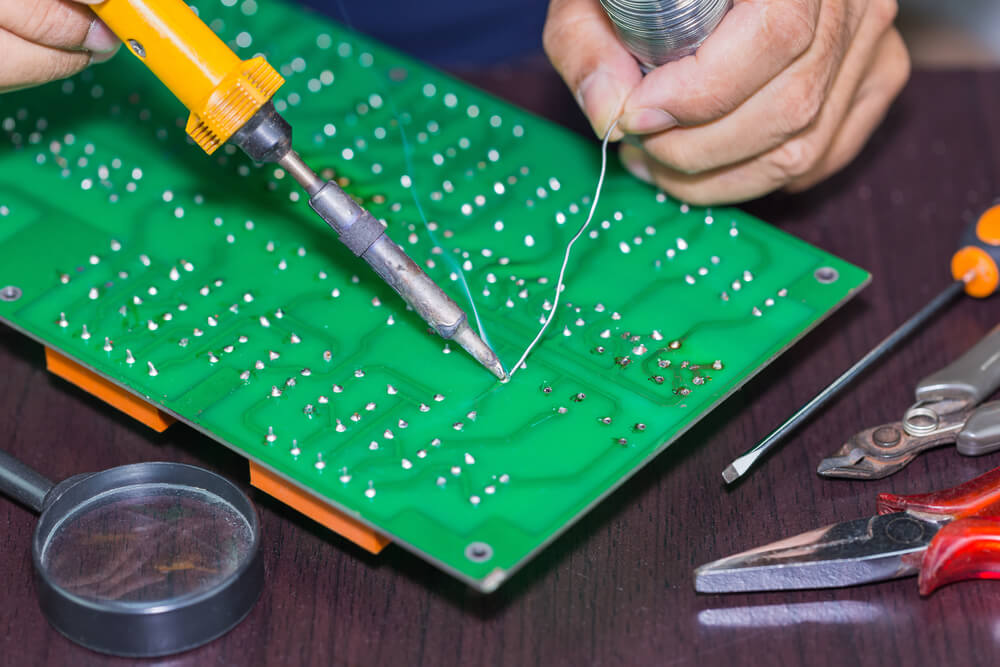
There are a couple of techniques available for soldering these components into through-hole circuit boards. We can use a hand solder and a soldering iron to apply the solder to the components’ leads and the PCB pads. This manual soldering approach prerequisites proper training to produce high-quality PCBs. Another prevalent option is called wave soldering. This involves passing the assembled PCB over a wave of molten solder, which wets and solders the component, which leads to the PCB.
Cleaning and Inspection
After soldering, the board undergoes a cleaning process to remove excess flux or any residue. Subsequently, it is inspected for faults or defects before being subjected to testing to ensure proper functionality. This is where inspection equipment like Automated Optical Inspection (AOI) systems and X-ray machines come into play, ensuring that the PCB boards are assembled perfectly.
AOI systems utilize cameras and sophisticated image processing algorithms to detect various assembly issues, including misaligned components, missing components, skewed components, and soldering defects. They thoroughly inspect the board’s surface and identify any anomalies affecting functionality.
On the other hand, X-ray inspection is beneficial for examining through-hole solder joints, especially those not visible from the surface of the PCB. This method ensures that all solder joints meet the necessary quality standards for reliability and performance.
Advantages of Through-Hole Technology
Durability:
Through-hole components are securely soldered to the PCB, making them resistant to damage and providing long-term reliability.
Higher Power Handling Capacity:
Through-hole components can handle higher voltage and current levels than surface mount counterparts due to their larger size.
Ease of Replacement:
When through-hole components fail or require upgrades, they are easier to replace due to their secure soldering and larger size, facilitating maintenance and repair processes.
Strong Mechanical Connection:
Through-hole components offer a robust mechanical connection to the PCB, making them suitable for high mechanical stress or vibration applications.
Drawbacks of Through-Hole Technology
Space Consumption:
Through-hole components occupy more space on the PCB, which can be challenging in compact or densely populated electronic designs, limiting compactness efforts.
Limited Availability:
With the industry’s shift towards surface mount technology, specialized components may have limited options for through-hole mounting or become unavailable altogether, potentially restricting design flexibility.
Parasitic Effects:
The longer lead lengths of through-hole components can introduce parasitic effects such as inductance and capacitance, limiting the maximum frequency or signal speed achievable in high-speed applications.
Mechanical Stress:
Components placed closer together in high-density designs can exacerbate mechanical stress issues in PCBs, leading to failures in the conductive pathways over time. This emphasizes the importance of careful design considerations to ensure long-term reliability.
Applications of Through Hole Technology
Here are some applications and examples of electronic devices that utilize through-hole assembly:
| Industry | Application area |
|---|---|
| Automotive industry | Employed in vehicle control systems, engine management, and infotainment systems. |
| Aerospace industry | Utilized in avionics, navigation systems, and communication equipment. |
| Industrial machinery | Found in industrial automation and control devices, such as PLCs (Programmable Logic Controllers), motor drives, and power supplies. |
| Medical devices | Utilized in including patient monitoring equipment, diagnostic tools, and surgical instruments. |
| Telecommunications | Commonly used in telecommunication equipment, especially for infrastructure components like switches, routers, and base stations. |
| Consumer electronics | Integrated into audio amplifiers, power supplies, connectors, etc. |
| Instrumentation and measurement devices | Employed in oscilloscopes, multimeters, data loggers, etc |
Surface Mount vs Through Hole Technology
Traditionally, through-hole technology has been the basis of electronic component assembly, valued for its durability, reliability, and ease of repair. However, with the emergence of surface mount technology (SMT), through-hole technology has encountered challenges. SMT offers smaller component sizes, higher component density, and faster assembly times, leading many electronic manufacturers to shift towards SMT for its efficiency and cost-effectiveness.
Here’s a comparison table highlighting the key differences between surface mount vs through hole based on different parameters/aspects:
| Parameter/Aspect | Through-Hole Technology | Surface Mount Technology (SMT) |
|---|---|---|
| Component Size | Through-hole components are larger and can include leads or pins that extend from the component body, consuming more space on the PCB. | SMT components are smaller, with no leads or pins. They rely on small contact points to connect to the PCB, allowing for greater PCB space utilization. |
| Component Density | Through-hole technology has lower component density, with a larger footprint for each component. | SMT has a higher component density, allowing for smaller PCBs and higher functionality in a smaller space. |
| Assembly Time | Through-hole technology typically requires more time to assemble due to manual or semi-automated assembly processes. | The fully automated process and smaller components make SMT faster to assemble. |
| Assembly Process | Through-hole components are typically inserted into the PCB manually or with semi-automated equipment. | SMT components are assembled with fully automated equipment, which places and solders components onto the PCB. |
| Assembly Cost | Through-hole technology is generally more expensive due to the manual or semi-automated assembly process and larger components. | SMT assembly is more cost-effective as a fully automated process with smaller components. |
| Rework and Repair | Through-hole components can be easier to rework or replace as it is easier to access the component leads. | Surface-mount technology (SMT) components, including Ball Grid Array (BGA) packages, require specialized rework stations and tools due to their smaller size, higher density, and unique design characteristics. |
| Thermal Performance | Through-hole components typically have better heat dissipation due to their larger size and efficient thermal coupling. | SMT components are more sensitive to heat due to their smaller footprint and limited thermal coupling |
| Vibration and Shock Resistance | Through-hole components have a higher mechanical strength and can withstand vibration and shock more effectively. | SMT components are smaller, making them more vulnerable to damage from vibration or shock. |
| When to Choose THT and SMT? | Preferred for applications requiring greater mechanical robustness and high-power handling capabilities. Easier for manual assembly, suitable for prototyping and small batch productions. | Suitable for compact designs and applications with space constraints. Better suited for automated assembly, ideal for mass production. Also, it is appropriate for miniaturized designs since it features smaller and lighter components. |
Recent Trends in Through-Hole Technology
Let’s dive into some exciting trends in through-hole technology shaping the future.
- Integration with Surface Mount Technology (SMT) is another major trend in through-hole technology. Engineers and manufacturers are finding ways to combine the best of both worlds by integrating through-hole and SMT components on the same circuit board. This hybrid approach offers the flexibility and reliability of through-hole technology combined with the efficiency and compactness of surface mount soldering. The result? More sophisticated devices that are both powerful and compact.
- Selective soldering has become a notable trend in Through-Hole Technology due to its precision and efficiency. This method enables targeted soldering, reducing heat exposure to sensitive components and minimizing thermal stress. As electronic assemblies grow more complex, selective soldering offers manufacturers flexibility in meeting quality standards while optimizing production. Its ability to accommodate diverse board layouts and component configurations makes it a valuable technique in modern THT assembly processes, ensuring reliability and efficiency.
These trends in through-hole technology showcase the relentless pursuit of innovation and improvement in the electronics industry.
As we look to the future of electronics assembly, it’s exciting to envision how new components, techniques, and innovations will shape the landscape of through-hole technology. Despite the growing popularity of surface mount technology (SMT), through-hole technology continues to hold its ground by complementing a broad set of industry needs and requirements.
When deciding between through-hole and SMT for your project, it’s not just about weighing the pros and cons—it’s about understanding the nuances of your specific application and finding the alignment with both options. Adding to your product demands, factors like cost-effectiveness, assembly efficiency, and reliability must also be considered.
Maybe if you are looking for a full-fledged partner to simplify your electronics design and manufacturing challenges, you are in the right place now. SRM Tech, as a comprehensive electronics value-chain partner, can help you navigate the intricacies of electronic product development and deliver top-notch products to the market. Our expertise and infrastructure can facilitate significant value addition in key areas like electronic product design, prototyping, fabrication, assembly, testing, and validation. Focusing on quality, reliability, and meeting industry standards, we enable our clients to streamline their electronics manufacturing process while ensuring cost-effectiveness and product success in the market.
Please connect with our team to learn more about our electronics manufacturing services and how we can transform your manufacturing needs with latest technology trends and best practices.